Question
Describe
the significance of h parameters
Draw
the simplest transistor amplifier circuit and explain the function of each
component
Answer
Every
linear circuit having input and output terminals can be analysed by four
parameters (one measured in ohm, one in mho and two dimensionless) called
hybrid or h Parameters.
[A
linear circuit is one in which resistances, inductances and capacitances remain
fixed when voltage acros-them changes.]
Hybrid
means "mixed". Since these parameters have mixed dimensions, they are
called hybrid parameters.
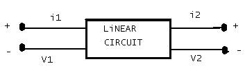
It
can be proved by advanced circuit theory that voltages and currents in Fig.
26.1 can be related by the following sets of equations:
V1 = h11 i1
+h12 v2
... (i)
i1 = h21 i12 + h22 V2
■ ■ ■ (ii)
In
these equations, the hs are fixed constants for a
given circuit and are called h parameters. Once these parameters are known, we
can use equations (i) and (ii) to find the voltages
and currents in the circuit. If we look at eq.(i), it is clear that *h1 has the dimension of ohm and h12
is dimensionless. Similarly, from eq. (ii), h21 is dimensionless and h22 has
the dimension of mho. The following points may be noted about h parameters :
(i) Every linear circuit has four h parameters
; one having dimension of ohm, one having dimension of mho and two
dimensionless.
(ii)
The A parameters of a given circuit are constant. If we change the circuit, h
parameters would also change.
Notice
in figure that the emitter-base battery has been eliminated and the bias
resistor R B has been inserted between the collector and the base. Resistor RB
provides the necessary forward bias for the emitter-base junction. Current
flows in the emitter-base bias circuit from ground to the emitter, out the base
lead, and through R B to V CC. Since the current in the base circuit is very
small (a few hundred microamperes) and the forward resistance of the transistor
is low, only a few tenths of a volt of positive bias will be felt on the base
of the transistor.
However,
this is enough voltage on the base, along with ground on the emitter and the
large positive voltage on the collector, to properly bias the transistor.
With
Q1 properly biased, direct current flows continuously, with or without an input
signal, throughout the entire circuit. The direct current flowing through the
circuit develops more than just base bias; it also develops the collector
voltage (VC) as it flows through Q1 and R L. Notice the collector voltage on
the output graph. Since it is present in the circuit without an input signal,
the output signal starts at the VC level and either increases or decreases.
These
dc voltages and currents that exist in the circuit before the application of a
signal are known as QUIESCENT voltages and currents (the quiescent state of the
circuit). Resistor RL, the collector load resistor, is placed in the circuit to
keep the full effect of the collector supply voltage off the collector. This
permits the collector voltage (VC) to change with an input signal, which in
turn allows the transistor to amplify voltage.
Without
RL in the circuit, the voltage on the collector would always be equal to VCC.
The coupling capacitor (CC) is another new addition to the transistor circuit.
It is used to pass the ac input signal and block the dc voltage from the
preceding circuit. This prevents dc in the circuitry on the left of the
coupling capacitor from affecting the bias on Q1. The coupling capacitor also
blocks the bias of Q1 from reaching the input signal source.
The
input to the amplifier is a sine wave that varies a few millivolts
above and below zero. It is introduced into the circuit by the coupling
capacitor and is applied between the base and emitter. As the input signal goes
positive, the voltage across the emitter-base junction becomes more positive.
This in effect increases forward bias, which causes base current to increase at
the same rate as that of the input sine wave. Emitter and collector currents
also increase but much more than the base current. With an increase in
collector current, more voltage is developed across R L. Since the voltage
across RL and the voltage across Q1 (collector to emitter) must add up to VCC,
an increase in voltage across RL results in an equal decrease in voltage across
Q1.
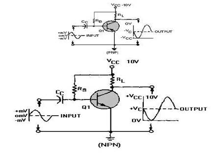
Figure—The basic transistor amplifier.
Therefore,
the output voltage from the amplifier, taken at the collector of Q1 with
respect to the emitter, is a negative alternation of voltage that is larger
than the input, but has the same sine wave characteristics. During the negative
alternation of the input, the input signal opposes the forward bias. This
action decreases base current, which results in a decrease in both emitter and
collector currents. The decrease in current through R L decreases its voltage
drop and causes the voltage across the transistor to rise along with the output
voltage. Therefore, the output for the negative alternation of the input is a
positive alternation of voltage that is larger than the input but has the same
sine wave characteristics.
By
examining both input and output signals for one complete alternation of the
input, we can see that the output of the amplifier is an exact reproduction of
the input except for the reversal in polarity and the increased amplitude (a
few millivolts as compared to a few volts). The PNP
version of this amplifier is shown in the upper part of the figure. The primary
difference between the NPN and PNP amplifier is the polarity of the source
voltage. With a negative VCC, the PNP base voltage is slightly negative with
respect to ground, which provides the necessary forward bias condition between
the emitter and base.
When
the PNP input signal goes positive, it opposes the forward bias of the
transistor. This action cancels some of the negative voltage across the
emitter-base junction, which reduces the current through the transistor.
Therefore, the voltage across the load resistor decreases, and the voltage
across the transistor increases. Since VCC is negative, the voltage on the collector
(VC) goes in a negative direction (as shown on the output graph) toward -VCC
(for example, from -5 volts to -7 volts). Thus, the output is a negative
alternation of voltage that varies at the same rate as the sine wave input, but
it is opposite in polarity and has a much larger amplitude. During the negative
alternation of the input signal, the transistor current increases because the
input voltage aids the forward bias. Therefore, the voltage across RL
increases, and consequently, the voltage across the transistor decreases or
goes in a positive direction (for example: from -5 volts to -3 volts).
This
action results in a positive output voltage, which has the same characteristics
as the input except that it has been amplified and the polarity is reversed. In
summary, the input signals in the preceding circuits were amplified because the
small change in base current caused a large change in collector current. And,
by placing resistor RL in series with the collector, voltage amplification was
achieved.