Question
By means of a schematic circuit diagram, illustrate
the peak rectifier.
If the supply voltage is v(t)
=Vm Sin wt, what is the voltage across the load
resistor?
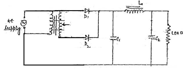
The above figure shows a full wave rectifier with a filter
arrangement
Diode D1 will conduct in +ve half
wave cycle, D2 in –ve half wave cycle
So the current through load will be in same direction but
pulsating or ripple are high with fluctuating D.C.
Thus we introduce filter to reduce these variation in voltage.
The filter arrangement has capacitance C1 across the rectifier, coil L in series and capacitor C2 across the
load.
The filtering action i.e. mentioned as follow
Filter capacitor C1 – offers low reactance to AC component of
rectifier O/P, while it offer infinite reactance to DC component
Therefore C1 bypasses an appreciable amount of AC component
while DC component continue its way to L.
Choke L – offer high reactance to AC component while almost o
reactance to DC components there fore it allows DC parts to flow through while
blocking AC component
Filter capacitor C2 – bypasses the AC component which the
choke has failed to block.
Therefore only DC component appear across the load and this
is desirable.
If supply voltage is V = Vm Sin wt
The O/P will be Vo – Vrmc = Vm / √2